

Two-Dimensional Semiconductor Innovation
Deposition equipment, process, and materials for wafer-scale 2D semiconductor manufacturing
01ABOUT TDS Innovation
Revolutionizing Next-Generation AI Computing with 2D Semiconductors
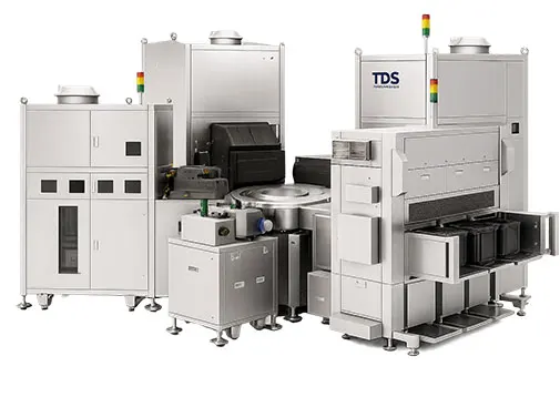
TDS Innovation develops deposition equipment, process, and materials technologies for the mass production of two-dimensional (2D) semiconductors — the next-generation channel material that will carry the industry beyond the limits of silicon scaling.
With atomically thin structures and outstanding electrical properties, 2D semiconductors are emerging as the channel material of choice for high-density, 3D-stacked, low-power, and high-performance devices.
Our proprietary Crystal Layer Deposition (CLD) process and equipment technology delivers high-quality 2D semiconductors at wafer scale, opening the door to heterogeneous integration with silicon and monolithic 3D integration.
02HISTORY
Moving fast, building deep
Since our founding, we have secured funding, certifications, and national programs that lay the groundwork for 2D semiconductor mass production.
2024
Company founded
Seed 1 funding round
R&D center established; certified as a venture company
Selected for the Deep-Tech TIPS program
2025
Named one of KAIST's 14 Future-Leading Technologies
Selected as a KODIT "First Penguin" company; certified as a materials, parts & equipment specialist
Seed 2 funding round
Minister of SMEs and Startups Award (Venture Startup Merit); designated as an alternative military service company
2026
Selected for IBK Chang-gong Daejeon (9th cohort)
Selected for DIPS (Super-Gap Startup Program)
Minister of SMEs and Startups Award (Innovative Startup)
Selected for Scale-up TIPS (Specialized track)
Pre-A funding roundLatest
03TECHNOLOGY
Across the whole wafer, one atomic layer at a time
Crystal quality, 3D conformality, and low-temperature processing — three barriers to 2D semiconductor manufacturing, solved on a single deposition platform.
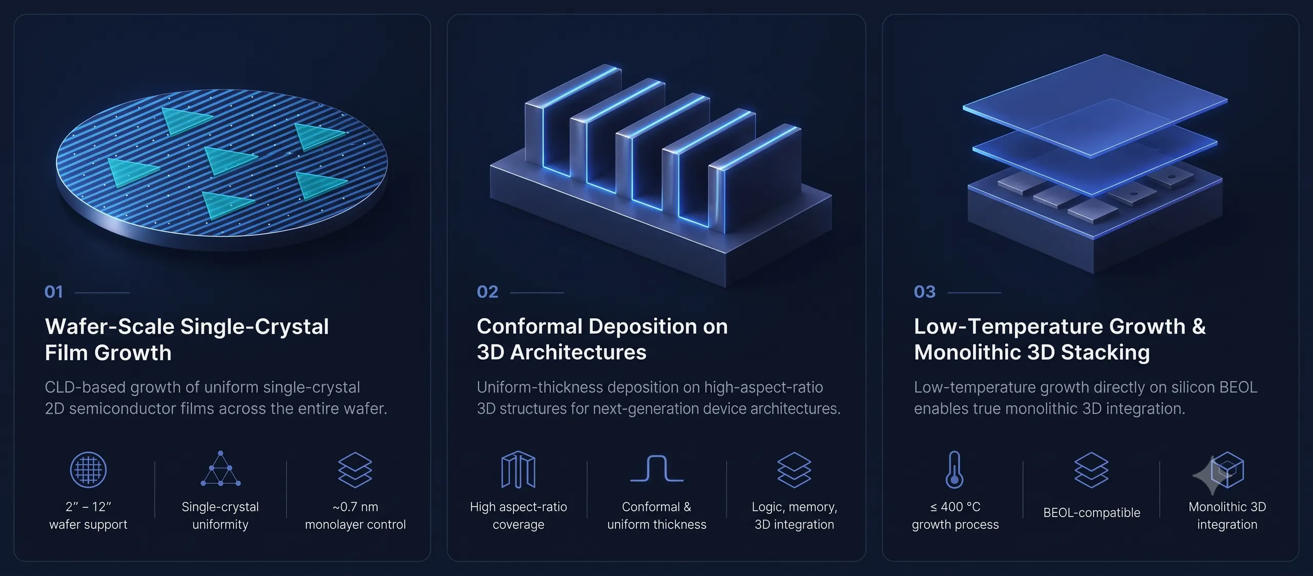
01. Wafer-Scale Single-Crystal Film Growth
CLD-based growth of uniform single-crystal 2D semiconductor films across the entire wafer.
02. Conformal Deposition on 3D Architectures
Uniform-thickness deposition on high-aspect-ratio 3D structures for next-generation device architectures.
03. Low-Temperature Growth & Monolithic 3D Stacking
Low-temperature growth directly on silicon BEOL enables true monolithic 3D integration.
Core technology
CLD · Crystal Layer Deposition
Our proprietary deposition technology controls everything from nucleation to crystal growth, with equipment, process, and materials engineered together.
04NEWS
Latest News
Updates from TDS Innovation, shared on LinkedIn.
01 / 09